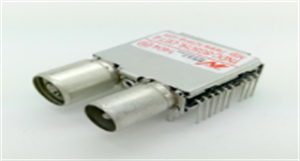
| Color | Silver |
DVB-C/T TV Receiver I2C-bus Full Band Tuner
FEATURES
• Full frequency range from 51 to 860MHz for DVB-C /T
• Low IF tuner concept
• Programmable channel Filter bandwidth
• Active LT & single supply voltage
• Fully I2C bus controlled
The half-NIM includes a full band tuner, an antenna loop through function (Active) and channel filtering for digital signals. It provides a low IF output after channel filtering to drive a DVB-C /T demodulator. Tuning, band switching and initialization are made via an I2C bus interface. The module is built on a low-loss printed circuit board carrying all the components in a metal housing frame with top and rear covers. The 2 aerial connectors are mounted on one frame side all other connections are made via pins at the bottom
|
NO |
SPECIFICATION |
|||||||||||||||||||||||||||||||||||||||||||||||||||||||||||||||||||||||||||||||||||||||||||||||||||||||||||||||||
|
3
|
RATINGS Environmental conditions
Limiting values under operational conditions The tuner can be guaranteed to function properly under the following conditions.
|
|||||||||||||||||||||||||||||||||||||||||||||||||||||||||||||||||||||||||||||||||||||||||||||||||||||||||||||||||
|
4
|
SPECIFICATION DATA If not otherwise stated the electrical performance refers to: 1.ambient temperature :22°C±2°C 2.relative humidity :60%±10% 3.supply voltages :3.3V±0.1V 4.IF-gain control voltage :1V max 5.RF-input termination :75ohms 6.RF-output termination :75ohms
|
|||||||||||||||||||||||||||||||||||||||||||||||||||||||||||||||||||||||||||||||||||||||||||||||||||||||||||||||||||||||||||||||||||||||||||||||||||||||||||||||||||||||
|
5
|
Antenna Active Loop through (TBD)
|
|||||||||||||||||||||||||||||||||||||||||||||||||||||||||||||||||||||||||||||||||||||||||
7.Application Information
The module contains of one programmable part, the tuner IC TDA18250HN, which can directly be programmed by the I2C-bus
7.1 Tuner
The source code for the TDA18250HN will be provided on request.
7.2 I2C Bus Requirements
The I2C implementation in the TDA18250HN follows the I2C bus specification, version 2.1, January 2000 as edited by Philips Semiconductors
7.3 I2C chip addresses
Write address: 0xC0, Read address: 0xC1
8. Electrostatic Discharge
8.1 Test
Each device must be capable of normal performance following its subjection to the following tests:
MIL STD 883C HBM
Test is performed with a voltage discharge from a 100 PF capacitor over a 1500 Ω series resistance in the discharge path. There is a direct contact between the test probe head and the unit under test, using the test points and conditions detailed below:
• Test to pins 1 through last pin : 3 successive ESD discharges of 2 KVDC between each pin and the
device frame.
IEC 1000-4-2
Test is performed with a voltage discharge from a 150 PF capacitor over a 330 Ω series resistance in the discharge path. There is a direct contact between the test probe head and the unit under test, using the test points and conditions detailed below:
•Test for antenna input socket 8 KVDC
•Test for antenna output socket 5 KVDC
8.2 Handling
Anyone handling a device must wear a properly grounded anti - static discharge bracelet to minimize ESD damage.
After each device is aligned and tested, it will be packed with anti - static poly-foam or material prior to transportation and storage. This protective foam is to remain in place until the device is assembled and soldered onto the receiver main board
9. Reliability Test Procedure & Conditions
Note: Room temperature = 25 °C ± 2 °C
9.1Heat Load Test
• Measure the DUTs at room temperature
•Load the DUTs into chamber of the following conditions:
Temperature = 60 °C
Period = 500 hrs
Cycle = 1,5 hrs on; 0,5 hrs off
Quantity = 10 pcs
•Cool-down 0,5 hr at room temperature, then perform functional test on DUTs within 1hr
•The test shall be continued to 1000 cycles for information only ( Optional )
9.2 Humidity Load Test
•Measure the DUTs at room temperature
• Load the DUTs into chamber of the following conditions:
Temperature = 40 5 °C
Period = 24 hrs
Cycle = constantly on
Quantity = 20 pcs
•Cool-down 0.5 hr at room temperature, then perform functional test on DUTs within 1hr
• Load the DUTs again into chamber of the following conditions:
Temperature = 40 5 °C
Humidity = 90 to 95 %
Period = 500 hrs
Cycle = 1,5 hrs on; 0,5 hrs off
Quantity = 20 pcs
•Cool down 0.5 hr at room temperature, then perform functional test on DUTs within 1hr
9.3Cold Test
•Measure the DUTs at room temperature
• Load the DUTs into chamber of the following conditions:
Temperature = - 20 5°C
Period = 500 hrs
Cycle = constantly on
Quantity = 10 pcs
•Warm up for 2 hrs at room temperature, then perform functional test on DUTs within 1hr
9.4Thermal Shock
•Measure the DUTs at room temperature
• Load the DUTs into chamber of the following conditions:
Temperature = - 25 °C for 60 min
↓ ↑
85 °C for 60 min
Period = 200 cycles
Power = power off
Quantity = 10 pcs
•Cool-down 0,5 hr at room temperature then perform functional test on DUTs within 1hr
9.5 Temperature Cycle Test
• Measure the DUTs at room temperature
• Load the DUTs into chamber of the following conditions:
Temperature = -5 °C for 16 hrs then 60°C for 8 hrs
Period = 500 hrs
Cycle = constantly on
Quantity = 10 pcs
•Cool down 0.5 hr at room temperature, then perform functional test on DUTs within 1hr
9.6Vibration Test
•Frequency: 3,5 Hz
• Vertical amplitude: 15 to 25 mm
•Duration: 1 hr
•Quantity: 1 carton
9.7Drop Test
•Packaged apparatus: < or = 50 kg
•Height: 32 … 50Kg: 0.5m
18 … 32Kg: 0.55m
10 … 18Kg: 0.65m
5 … 10Kg: 0.8m
•1 corner + 3 edges + 6 faces
•Quantity: 1 carton
9.8 Life Test
•Measure the DUTs at room temperature
• Load the DUTs into chamber of the following conditions:
Temperature = 60°C
Period = 500 hrs
Cycle = constantly on
Quantity = 20 pcs
•Cool down 0.5 hr at room temperature, then perform functional test on DUTs within 1hr